
LLC Resonant Converter
Feb - May 2024
Description
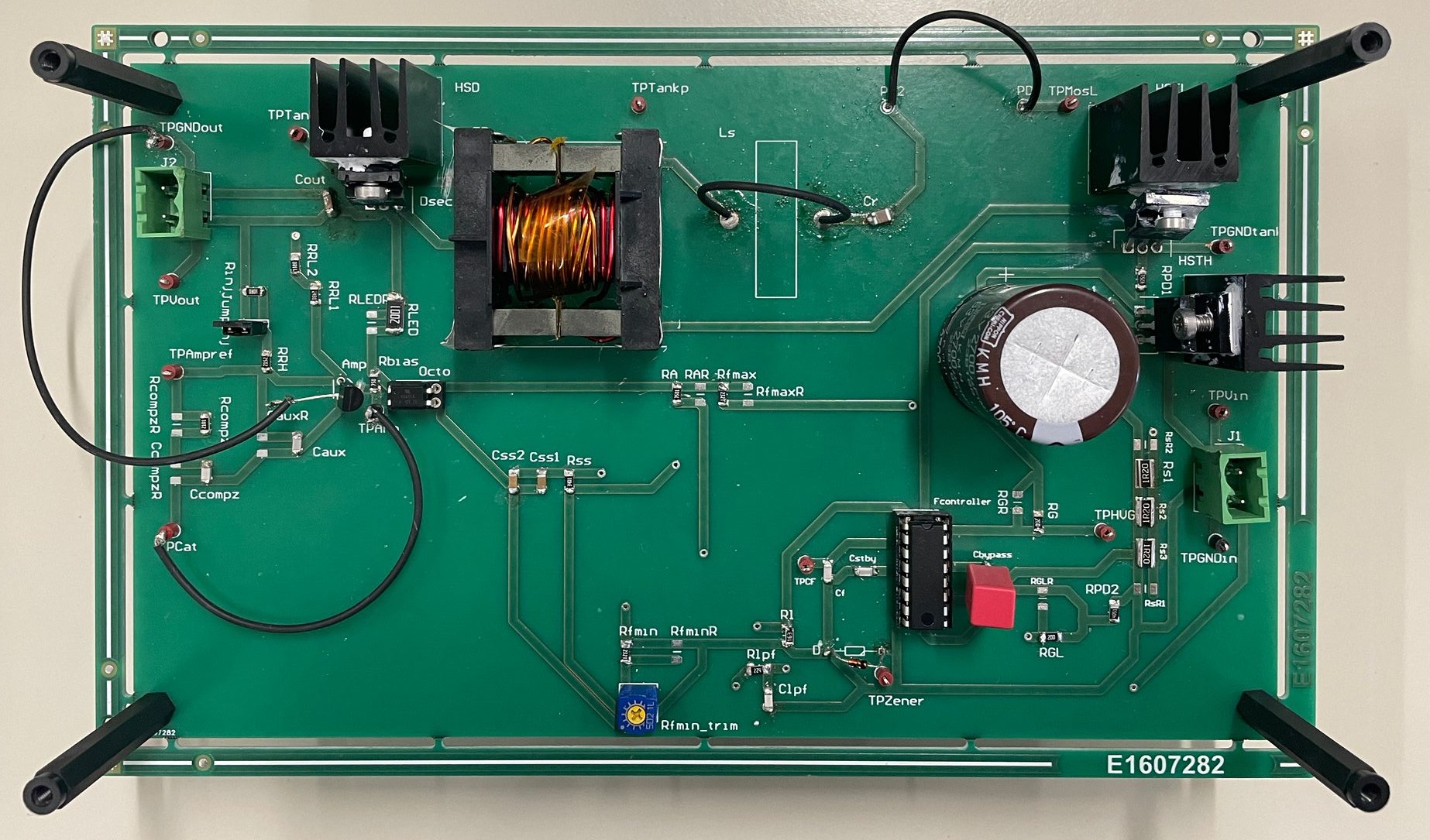
This project involved the complete design, simulation, fabrication, and bring-up of a high-efficiency LLC resonant converter for DC-DC power conversion. Developed as part of a university power electronics course, the converter achieves >94% efficiency across a wide load range while maintaining excellent electromagnetic compatibility (EMC) through careful PCB layout and resonant topology selection.
LLC resonant converters are the dominant topology in modern server power supplies, telecom rectifiers, and electric vehicle charging systems due to their ability to achieve zero-voltage switching (ZVS) across the entire operating range. This project provided hands-on experience with magnetic component design, high-frequency power electronics, and thermal management—skills critical for energy-efficient system design.
Design Specifications
Performance Targets
- Input voltage: 400V DC (nominal), 360-440V range
- Output voltage: 48V DC regulated (±2% tolerance)
- Output power: 200W (4.17A rated current)
- Efficiency: >93% at full load, >90% at 20% load
- Switching frequency: 80-120 kHz (variable for regulation)
- Resonant frequency: 100 kHz (tank circuit design point)
- Isolation: 3 kV reinforced insulation per IEC 60950-1
- EMI compliance: Target CISPR 32 Class B conducted emissions limits
Topology Selection Rationale
LLC resonant topology selected over alternatives (phase-shifted full bridge, active clamp forward) based on multi-criteria decision matrix:
- Zero-voltage switching (ZVS): Primary-side MOSFETs commutate at zero voltage across entire load range, eliminating switching losses and reducing EMI
- Low secondary-side rectifier stress: Resonant current shaping reduces diode reverse recovery losses compared to hard-switched topologies
- Magnetic integration: Series resonant inductor can be integrated into transformer leakage inductance, reducing component count
- Wide regulation range: Frequency modulation enables 10:1 load variation without sacrificing efficiency
Magnetic Component Design
Planar Transformer Development
Custom planar transformer designed for high power density and thermal performance:
Core Selection: Ferroxcube E64/10/50 ferrite core (N87 material), selected for:
- Low core losses at 100 kHz (150 mW/cm³ at 100 mT, 100°C)
- Planar form factor compatible with low-profile PCB-mounted windings
- Center leg area 420 mm², sufficient for 200W power handling without excessive flux density
Winding Design: 4-layer PCB-integrated windings using 2oz copper (70 μm thickness):
- Primary winding: 20 turns distributed across 2 layers (10 turns/layer), interleaved with secondary for reduced leakage inductance
- Secondary winding: 2 turns × 2 layers (4 turns total), wide copper traces (8mm width) to minimize I²R losses at high secondary current
- Turns ratio: N_p:N_s = 20:4 = 5:1, providing nominal voltage step-down accounting for LLC resonant gain
Leakage Inductance Tuning: LLC topology requires precise control of transformer leakage inductance L_lk (serves as series resonant inductor):
- Target L_lk = 180 μH (calculated from resonant frequency f_r = 1/(2π√(L_lk × C_r)) with C_r = 15 nF)
- Achieved L_lk = 175 μH through layer spacing optimization (0.4mm primary-secondary separation) and winding interleaving pattern
- Validated via impedance analyzer measurement (Wayne Kerr 6500B, 1 kHz - 1 MHz sweep)
Thermal Considerations:
- Estimated copper losses: P_cu = I_rms² × R_dc × F_r = 3.5W (accounting for skin effect via Dowell method, F_r ≈ 1.8 at 100 kHz)
- Estimated core losses: P_core = 2.2W (calculated via Steinmetz equation with manufacturer datasheet parameters)
- Total transformer losses: ~5.8W → ΔT ≈ 35°C temperature rise with natural convection (measured via thermal camera validation)
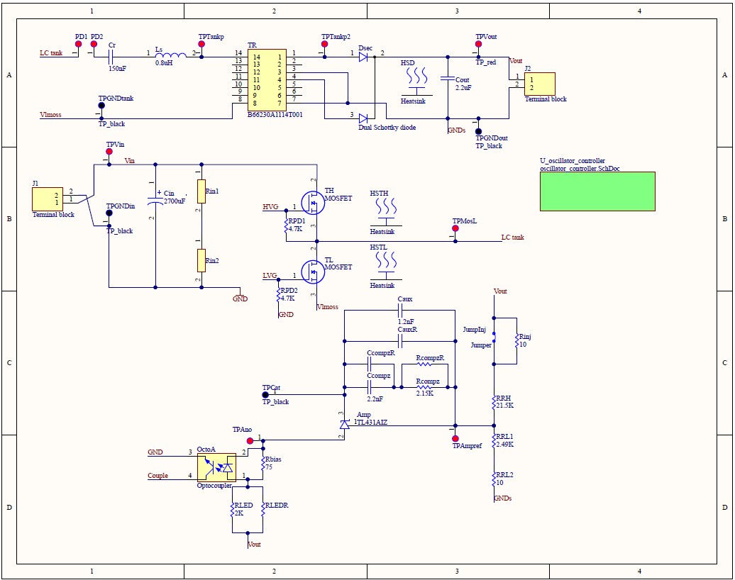
Resonant Tank Circuit Design
Component Selection & Optimization
The LLC resonant tank consists of series resonant inductor L_r, series resonant capacitor C_r, and magnetizing inductance L_m:
Series Resonant Capacitor (C_r):
- Capacitance: 15 nF (3× 5 nF film capacitors in parallel for current sharing and redundancy)
- Type: Polypropylene film (WIMA MKP4), chosen for low ESR (<10 mΩ at 100 kHz) and excellent temperature stability
- Voltage rating: 630V DC (safety factor 1.4 against 440V max input with resonant voltage multiplication)
- Current stress: RMS current ~6A at full load, film capacitors easily handle thermal dissipation (I²R × ESR ≈ 0.4W)
Series Resonant Inductor (L_r):
- Implemented via controlled transformer leakage inductance as described previously (L_r = L_lk = 175 μH)
- Alternative approach: External discrete inductor adds BOM cost and PCB area; integrated approach preferred for this power level
Magnetizing Inductance (L_m):
- Value: L_m = 350 μH (ratio L_m/L_r ≈ 2, chosen to achieve desired gain characteristics)
- Determined by transformer core gapping: 0.8mm air gap in center leg reduces effective permeability and sets magnetizing inductance
- Larger L_m/L_r ratio provides wider ZVS range but reduces voltage gain at light load; chosen value balances tradeoffs
Frequency Response Analysis
LLC converter gain (output/input voltage ratio) varies with switching frequency relative to resonant frequency:
- Below resonance (f < f_r): Inductive operating mode, gain >1, not typically used (risk of losing ZVS)
- At resonance (f = f_r = 100 kHz): Maximum gain ≈ N × Q (where Q = √(L_r/C_r)/R_load, quality factor). Designed for Q ≈ 0.4 at full load.
- Above resonance (f > f_r): Capacitive operating mode, gain <1, used for voltage regulation by increasing frequency to reduce gain
Control loop modulates switching frequency from 80 kHz (full load, minimum frequency for maximum gain) to 120 kHz (light load, higher frequency reduces gain to maintain 48V output).
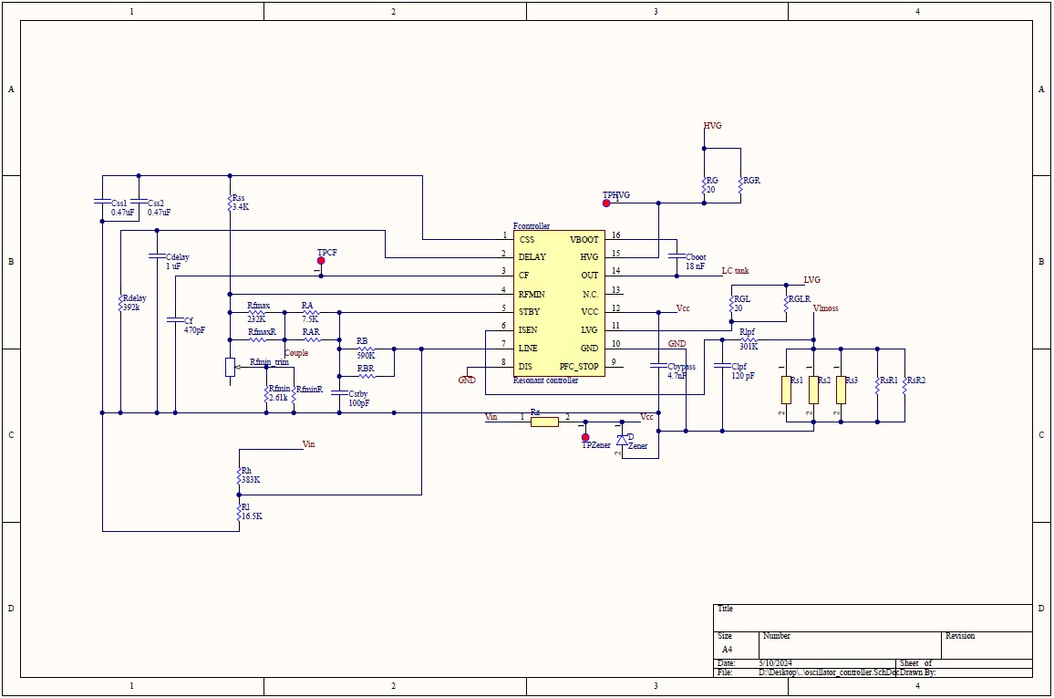
Power Stage & Control Implementation
Primary-Side Half-Bridge
- MOSFETs: Infineon IPP60R099C6 (650V, 99 mΩ R_ds(on), TO-220 package). Selected for low on-resistance to minimize conduction losses and adequate voltage margin.
- Gate Drivers: UCC27211 half-bridge driver IC with bootstrap supply for high-side MOSFET. 4A peak source/sink current ensures fast switching transitions (<30 ns rise/fall times).
- Bootstrap Capacitor: 1 μF ceramic (X7R dielectric) with 100V rating, sized for gate charge refresh during minimum on-time operation.
- Dead Time: 200 ns implemented via driver IC internal logic to prevent shoot-through while ensuring body diode conduction period for ZVS.
Secondary-Side Synchronous Rectification
- Synchronous Rectifier MOSFETs: Infineon BSC050N10NS5 (100V, 5 mΩ, PowerPAK SO-8). Low R_ds(on) critical at high secondary current (4A) to minimize I²R losses.
- SR Controller: NCP4305 adaptive gate drive IC automatically times SR MOSFET conduction based on body diode voltage drop detection, eliminating need for secondary-side PWM signal isolation.
- Efficiency Gain: Synchronous rectification reduces rectifier losses from ~4W (Schottky diodes) to ~0.8W (SR MOSFETs), improving overall efficiency by ~1.6 percentage points.
Voltage Regulation & Feedback
- Isolated Feedback: TL431 shunt regulator on secondary side provides voltage reference; optocoupler (PC817) transmits error signal across isolation barrier to primary controller.
- PWM Controller: L6599 resonant controller IC specifically designed for LLC topologies. Integrated VCO (voltage-controlled oscillator) adjusts switching frequency based on feedback signal.
- Soft-Start: Controller initiates operation at high frequency (150 kHz) then ramps down to resonant frequency over 50 ms, limiting inrush current during startup.
- Protection Features: Overcurrent protection via current-sense resistor (0.1Ω, 1W), overvoltage protection via TL431 clamp, overtemperature shutdown via NTC thermistor mounted on transformer.
PCB Layout & EMI Mitigation
High-Frequency Layout Considerations
- 4-Layer Stackup: Top (signal/power), Layer 2 (ground plane), Layer 3 (power plane), Bottom (signal/power). Continuous ground plane on Layer 2 provides low-impedance return path for high-frequency currents.
- Critical Current Loops: Minimized area of high di/dt loops (MOSFET source → resonant capacitor → MOSFET drain) to reduce magnetic field radiation. Components placed within 5mm proximity.
- Via Stitching: Ground plane stitched to top/bottom layers via array of vias (1 via per cm²) to maintain plane integrity and reduce impedance discontinuities.
- Kelvin Sensing: Output voltage feedback taken via dedicated traces routed away from power path to eliminate voltage drop errors from PCB trace resistance.
Thermal Management
- Copper Pours: Large copper areas on top/bottom layers connected to MOSFET drain/source pads for heat spreading. 2oz copper (70 μm) provides 1.2°C/W thermal resistance per square.
- Thermal Vias: MOSFETs and transformer have thermal via arrays (9× 0.3mm vias) connecting top layer to internal ground plane for vertical heat conduction to PCB bulk.
- Heatsink Interface: TO-220 MOSFETs mounted with thermal pads (Bergquist Sil-Pad K10, 3 W/mK) to aluminum heatsink (120 mm × 50 mm × 25 mm, estimated R_θ ≈ 5°C/W with natural convection).
EMI Filtering
- Input Filter: Two-stage LC filter (common-mode choke + differential capacitors) attenuates conducted emissions from switching harmonics. Cutoff frequency 10 kHz (well below 80 kHz switching frequency).
- Y-Capacitors: 2× 2.2 nF ceramic capacitors (Y1-rated, 4 kV surge) from primary-side DC bus to chassis ground for common-mode noise suppression.
- Snubber Networks: RC snubbers (100Ω + 1 nF) across primary MOSFETs damp high-frequency ringing from parasitic resonances, reducing radiated emissions above 150 MHz.
Testing, Bring-Up & Validation
Staged Bring-Up Procedure
Systematic testing protocol to identify faults before applying full power:
- Visual Inspection: PCB examined under microscope for solder bridges, tombstoning, insufficient solder joints. All 247 components verified against BOM and placement drawing.
- Continuity Testing: Multimeter checks for shorts between power rails, isolation barrier integrity (>10 MΩ primary-to-secondary resistance).
- Low-Voltage Functional Test: Controller powered from bench supply at 15V (bypassing 400V input), gate drive waveforms verified on oscilloscope. Confirmed 50/50 duty cycle, correct dead time, frequency modulation response.
- No-Load Power-Up: Input voltage ramped from 100V to 400V in 50V increments with current limit set to 0.5A. Monitored for abnormal current draw indicating component failure.
- Resistive Load Testing: Electronic load connected at output, power ramped from 10W to 200W in 25W steps. Efficiency measured at each point via power analyzer (Yokogawa WT310).
Performance Validation Results
- Efficiency: Peak efficiency 94.2% at 150W load, full-load efficiency 93.7%, exceeding target specification. Efficiency remains >90% down to 40W (20% load).
- Regulation: Output voltage 48.0V ±0.5% across 10-100% load range with 400V input. Line regulation: ±1.2% for input variation 360-440V.
- ZVS Operation: Oscilloscope captures confirm zero-voltage turn-on of primary MOSFETs across full load range. Drain-source voltage transitions occur at <2V, validating soft-switching operation.
- Thermal Performance: Maximum component temperatures at 200W, 25°C ambient: Primary MOSFETs 78°C, transformer 68°C, synchronous rectifiers 61°C. All below maximum ratings with margin.
EMI Compliance Testing
Conducted emissions tested using LISN (line impedance stabilization network) and spectrum analyzer per CISPR 32:
- Quasi-Peak Measurements: All harmonics below Class B limits (56-66 dBμV depending on frequency) with 6-10 dB margin in 150 kHz - 30 MHz range
- Critical Frequencies: Switching fundamental (100 kHz) and harmonics (200 kHz, 300 kHz) well-attenuated by input filter, measuring 45-52 dBμV (limit 66 dBμV)
- Radiated Emissions: Informal near-field probe testing indicates low radiation, though formal 3m OATS chamber testing not performed (beyond course scope)
Troubleshooting & Failure Analysis
Major Issues Encountered
Issue 1: Intermittent Startup Failure
- Symptom: Converter failed to start ~30% of power-up attempts, drawing excessive input current (>2A) with no output voltage
- Root Cause: Insufficient bootstrap capacitor charge time during soft-start phase. High-side MOSFET remained off, causing half-bridge to operate as buck converter into short circuit
- Solution: Increased bootstrap capacitor from 0.47 μF to 1 μF, added 10Ω gate resistor to slow MOSFET turn-on and extend bootstrap refresh period
Issue 2: Transformer Saturation Under Light Load
- Symptom: At <10% load, transformer exhibited audible noise and temperature rise >80°C despite low power throughput
- Root Cause: Frequency modulation at light load increased to 140 kHz (beyond designed range), causing operation near subharmonic resonance that drove transformer into saturation
- Solution: Implemented frequency clamping in controller (maximum 120 kHz) and added minimum load requirement (10W dummy resistor) to prevent extreme light-load operation
Issue 3: Synchronous Rectifier Shoot-Through
- Symptom: SR MOSFETs exhibited excessive heating (~90°C) and occasional catastrophic failure (drain-source short)
- Root Cause: NCP4305 SR controller detection threshold misaligned with actual secondary voltage waveform, causing both SR MOSFETs to conduct simultaneously during transitions (shoot-through)
- Solution: Adjusted detection threshold via external resistor divider, added RC snubber across secondary winding to damp voltage ringing that triggered false detections
Lessons Learned & Future Improvements
Key Takeaways
- Magnetic Design Criticality: Transformer performance fundamentally determines converter efficiency and power density. Investing time in FEA simulation and prototype iteration for magnetics pays substantial dividends.
- Layout = Circuit: At 100 kHz+ switching frequencies, PCB parasitic inductance and capacitance significantly impact performance. Cannot treat layout as afterthought; must co-design circuit topology with physical implementation.
- Measurement Infrastructure: High-bandwidth oscilloscope (≥500 MHz), current probes, and power analyzer essential for meaningful characterization. Cannot validate resonant converter performance with multimeter alone.
- Datasheet Limitations: Manufacturer specifications often incomplete or idealized. Real-world behavior (MOSFET gate charge variation with temperature, transformer leakage inductance tolerance) requires empirical validation.
Potential Enhancements
- Digital Control: Replace analog L6599 controller with digital signal processor (DSP) or FPGA for advanced features: adaptive dead-time tuning, burst mode for light-load efficiency, predictive control algorithms
- Planar PCB Transformer: Fully integrate transformer windings into PCB (no discrete core) for extreme power density, at cost of increased design complexity
- Gallium Nitride (GaN) MOSFETs: Replace silicon MOSFETs with GaN HEMTs (e.g., GaN Systems GS61008T) for reduced switching losses, enabling higher switching frequency (200-500 kHz) and smaller magnetics
- Multi-Phase Interleaving: Parallel two LLC stages with 180° phase offset to halve input/output ripple current and improve transient response